Ledger gate. This document is on the compute-and-storage ledger and describes no sensing product. It is never put in front of a sensing-ledger counterparty, and no sensing document references it. Every compute statement here is conditional on experiments that have not been run: under the group’s own standing rule, a negative E1 on species means no computing claim is ever made.
What OPALBLACK is, and the constraint it addresses
Pair silicon with protons
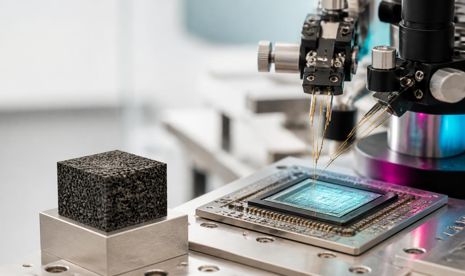
Silicon is the finest logic substrate ever built and it should stay exactly where it is. The opportunity is beside it — and the laboratory furthest ahead in protonic devices reached the same conclusion, building its leading result to run on silicon, at nanosecond speed, at room temperature. Here is what OPALBLACK is, where the room beside the chip has opened, and why an oxide grown in a bath is well placed to occupy it.
The third computing substrate
After electrons. After photons. Protons.
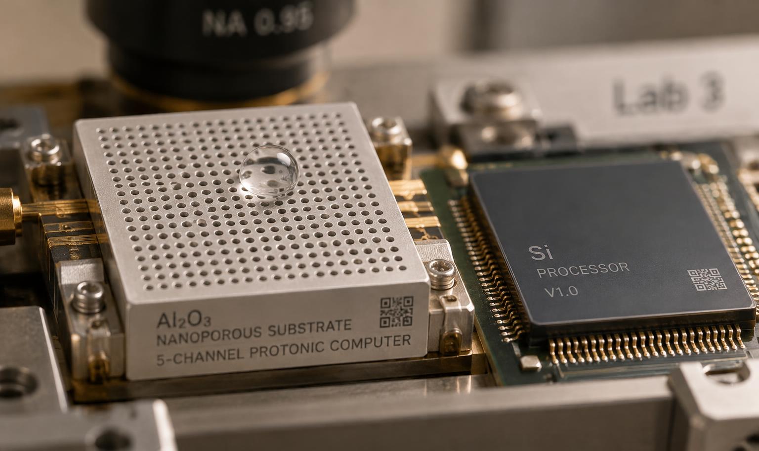
OPAL™ — Oxide-Mediated Protonic Analogue Logic. The world's first five-channel protonic computer. Built from aluminium and water. Sovereign. Self-powered.
OPAL Protoni™ computers sit alongside silicon chips: silicon handles high-speed digital processing; the protonic layer handles low-cost, persistent, long-timescale learning — memory and compute in the same oxide, without a separate RAM bus.
Visit our sister site, protonicopal.com, to see how it works →
Stated plainly
OPALBLACK is nanoporous anodic aluminium oxide, engineered as a proton-transport medium and read electrically.
The material is seventy years old
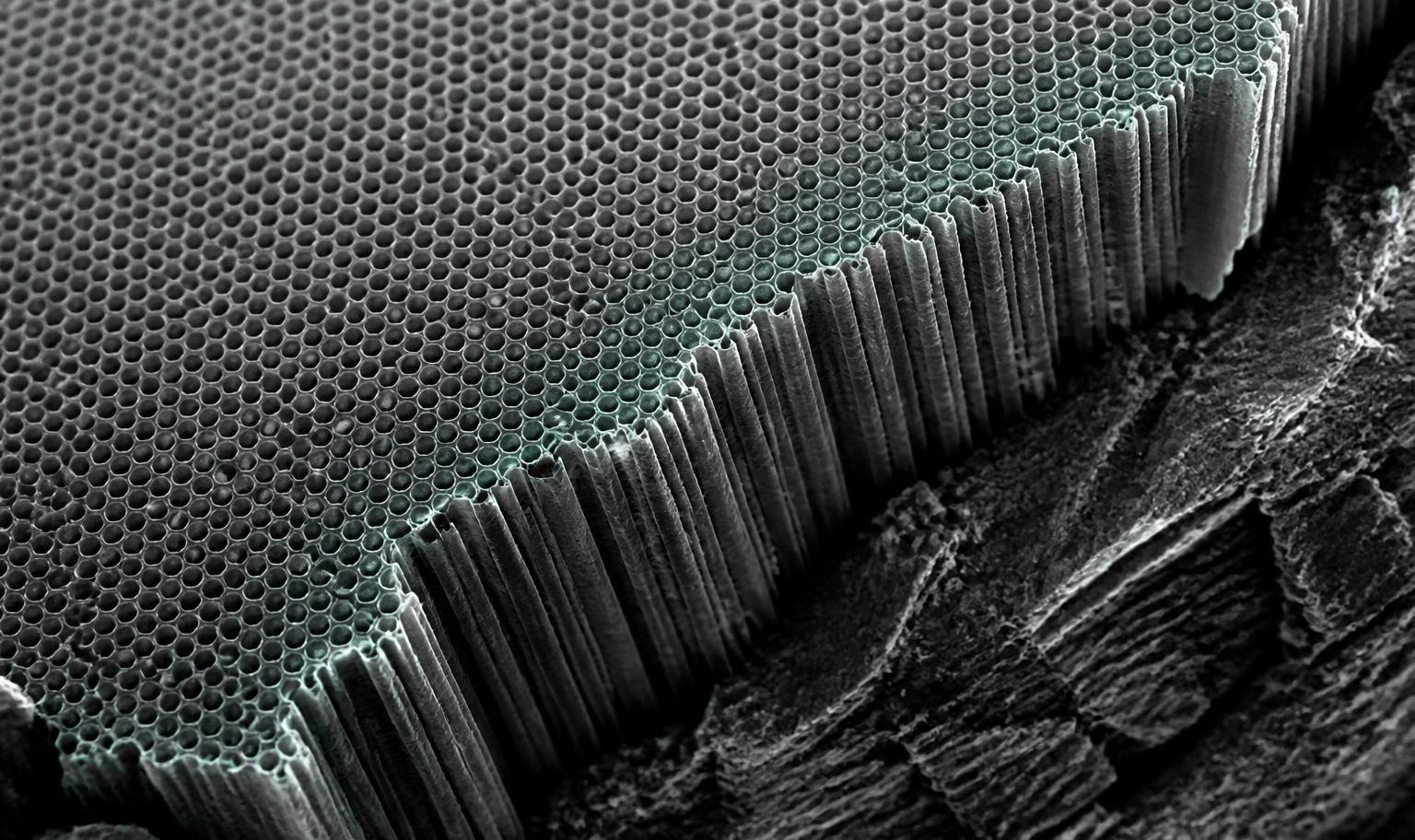
Anodising grows a controlled porous oxide skin on aluminium by passing current through it in a bath. It is done at industrial scale, everywhere, today. Nothing about making the layer is exotic, and nothing about it requires a fab.
What is engineered is the pore structure
Pore geometry, sealing state and zonal definition across one part — so that different regions of the same oxide carry different function. That arrangement is what the group has filed on. Filed, not granted, and not searched by an authority.
The carrier is a proton, not an electron
In porous anodic alumina, conduction runs by electron tunnelling when dry and protonically when humid. That is established physics, published in 1984 and repeatedly confirmed since. It is not the group's discovery and is never presented as one.
The same oxide, read at two depths
Read shallow, it reports what a surface has been exposed to — that is a different ledger, sold as a sensor that stores nothing. Read deep, it is a candidate for holding and modulating state. Both can be true of different experiments. They are never sold to the same buyer.
The compute proposition in one sentence: An aluminium-oxide layer that holds and modulates analog state by moving protons a short distance, made by anodising rather than by lithography, working alongside silicon logic rather than in place of it. Three experiments stand between that hypothesis and an answer — and all three run on consumables and equipment the group already owns.
Keep silicon for
- Logic, arithmetic and control
- The memory hierarchy the industry already has
- Everything that needs a foundry’s precision
- The processor a protonic layer still sits beside
Pair protons for
- Holding analog weights a short distance from the die
- Work that should not join the wafer queue
- A bath process on a seventy-year equipment base
- One narrow job, done well, next to the chip
We do not dump silicon. We do not claim it is running out. We pair it with a proton-transport medium so that some of the work that currently competes for a 2nm slot, a CoWoS slot and an HBM allocation can be done on an oxide grown in a bath. The rest of this sheet is why that pairing is the correct posture, and what would make us drop it.
Why this work exists
01
The best chips are scarce, and they are allocated rather than sold
A 2nm wafer is reported at about US$30,000, against roughly US$18,000–22,000 for 3nm on current analyst models. That capacity is booked into 2028. HBM3E memory is effectively sold out for 2026. Three separate allocations — a wafer slot, a packaging slot, a memory allocation — must line up before a single accelerator ships.
02
AI runs on very large data centres, and they are being built at speed
Data-centre electricity consumption rises from 415 TWh in 2024 to 945 TWh in 2030 on the IEA base case — slightly more than Japan consumes today — growing at 15 per cent a year, more than four times faster than every other sector combined. Accelerated servers, the AI workload specifically, grow at 30 per cent a year.
03
That load is expensive, and it lands in a few places at once
About half of all US electricity demand growth to 2030 comes from data centres; the country is set to use more electricity processing data than making all energy-intensive goods combined. Unlike electric vehicles, data centres cluster — so the binding problem is grid integration in specific locations, not aggregate national share.
04
And they drink — twice
About 222 billion litres consumed directly for cooling in 2025, heading for 644 billion litres by 2030. Then the larger figure almost nobody counts: roughly 211 billion gallons — some 800 billion litres — consumed indirectly in 2023 generating the electricity for US data centres alone, at about 1.2 gallons per kilowatt-hour. Water is spent at the cooling tower and again at the power station.
The question this programme asks
1%
What if we could take one per cent off it?
Not a revolution. Not a replacement. One per cent of the 2030 projection — the smallest number still worth the arithmetic. Nobody has to believe in a revolution for these numbers to be worth chasing, and no single technology has to deliver it alone.
Move the levers. The arithmetic is live.
945 TWh is the IEA 2030 base case. The tariff is ours, not a sourced figure. 1.2 gal/kWh is the US national average for thermal generation — a wind-and-solar grid carries almost none of it.
9.45 TWh
of electricity a year, unspent.
From a sourced figure~43bn L
of water left in the ground, at the power station.
Derived — working belowUS$756m
a year in electricity, at the tariff you set.
Modelled — stated assumption6.7×
more water saved than taking the same share off direct cooling (~6.4bn L).
Derived — working belowThe working, so it can be checked
945 TWh × 1.00% = 9.45 TWh. At 1.20 gal/kWh: 9.45 × 10⁹ kWh × 1.20 = 11.3 billion gallons = ~43bn L. Against direct cooling: 644 billion litres × 1.00% = ~6.4bn L. Ratio 6.7×. At US$0.08/kWh: US$756m.
One per cent is chosen deliberately. A device class that carries one narrow job — holding analog weights beside the processor rather than replacing it — only needs to be good at that job. And the honest scale, because it sharpens rather than softens the case: at 15 per cent annual growth, the sector replaces 9.45 TWh in about twenty-four days. That is precisely why efficiency has to come from a structurally different device rather than a better version of the same one — and why the manufacturing route matters as much as the physics.
The opening
Leading-edge silicon is precious — which is exactly what creates room beside it
Every figure below is public and dated. None is the group’s. Wafer prices are analyst estimates: TSMC does not disclose them.
$30,000
per 2nm wafer, on analyst estimates of TSMC's price — against roughly $18,000–22,000 for 3nm. TSMC does not disclose list prices.
TrendForce / Silicon Analysts, 2025–26
2028
how far 2nm capacity is reported booked. Access is allocated to a handful of lead customers, not purchased on an open market.
Supply-chain reporting, 2026
Sold out
HBM3E for 2026. CoWoS advanced packaging is fully booked through the same year. One missing allocation ships nothing.
Silicon Analysts, 2026
3
things must line up for one AI accelerator: a wafer slot, a CoWoS packaging slot, and an HBM allocation.
Industry structure, checkable today
Supply, not just price. TSMC’s 2nm capacity has been reported booked into 2028. Advanced nodes run at full allocation while legacy nodes remain underutilised — the shortage is specific to the leading edge, not general. HBM3E, the memory in most current AI accelerators, is described as effectively sold out for 2026, and CoWoS advanced packaging still books out even after years of capacity growth.
What this establishes. Leading-edge logic and the memory beside it are capital-rationed, concentrated in very few suppliers, and access to them is allocated rather than purchased. That is a durable and well-documented opening for anything that does useful work without joining the queue, and it is the opening this programme is aimed at.
And the honest bound on it. None of this means silicon is running out, that mature nodes are constrained, or that any alternative is ready to absorb displaced demand — legacy capacity sits underutilised. The constraint is a narrow and expensive corridor at the top. Stating that bound plainly is what makes the opening above worth taking seriously.
The demand
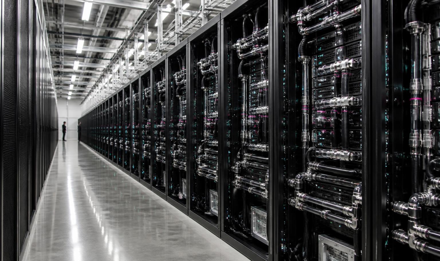
Data-centre load is growing faster than anything else on the grid
The International Energy Agency’s Energy and AI analysis is the authoritative public source, and it is worth quoting precisely rather than dramatically. The 2026 update keeps the same trajectory.
945 TWh
projected data-centre electricity consumption in 2030, from 415 TWh in 2024 — slightly more than the entire electricity consumption of Japan today.
IEA, Energy and AI, 2025 base case
15% a year
growth in data-centre electricity consumption 2024–2030 — more than four times faster than electricity consumption growth in all other sectors combined.
IEA base case
~50%
of all US electricity demand growth to 2030 comes from data centres. The US is set to use more electricity processing data than making all energy-intensive goods combined.
IEA, 2025
30% a year
growth in electricity used by accelerated servers specifically — the AI workload — against 9 per cent for conventional servers.
IEA base case
The honest scale, and the sharper argument inside it
The argument that holds is concentration, and the IEA makes it directly: unlike electric vehicles, data centres cluster in specific locations, so grid integration — not aggregate share — is the binding problem. That is a far better argument for this work than a global-load story would be, because it is the one that survives scrutiny. For completeness: data centres reach about 3 per cent of global electricity demand by 2030, under 10 per cent of the overall increase, behind electric vehicles and air conditioning. We use the concentration framing throughout and never the planetary one.
The multiplier
Every watt saved is paid for twice
The sharpest fact in this document sits here, and it is not the one usually quoted.
222bn L
consumed directly for data-centre cooling in 2025, projected to nearly triple to 644 billion litres a year by 2030 without efficiency gains.
Rystad Energy, 2026
211bn gal
the indirect water footprint of US data centres in 2023 — water consumed generating their electricity. Roughly 1.2 gallons per kWh nationally.
LBNL 2023, via IEEE Spectrum / EESI
12×
how much larger the US indirect water figure is than the US direct cooling figure (211 billion gallons against about 17 billion). Most of the water never appears on a WUE dashboard.
Derived from LBNL 2023
1.2 gal
consumed per kilowatt-hour by the US electric power sector. A grid running on wind and solar carries almost no thermal water cost; a thermal grid carries almost all of it.
IEEE Spectrum, citing US power-sector intensity
The fact that matters. Direct cooling water worldwide was about 222 billion litres in 2025. The indirect water footprint of US data centres alone — water consumed at the power stations supplying them — was around 211 billion gallons in 2023, roughly 800 billion litres. The water cost of the electricity dwarfs the water cost of the cooling, and it is not on anyone’s Water Usage Effectiveness dashboard.
This is the strongest available argument for working on compute energy rather than on cooling. A watt not spent is paid for twice: once at the meter, and again at the power station’s cooling tower. Efficiency measures that address only site water — closed-loop cooling, engineered fluids, direct-to-chip — leave the larger figure untouched.
The bounds of the claim. These figures are not commensurable without care: operators define water usage effectiveness differently, some report withdrawal rather than consumption, and the indirect figure depends entirely on the generation mix supplying a given site. A grid running on wind and solar carries almost no thermal water cost. The claim that survives all of that is narrow and sufficient: where the grid is thermal, reducing compute energy reduces water more than reducing cooling water does.
The lineage
Protonic computing is not a new idea, and that is the point
A proposal that needs a new physics is a proposal that needs a miracle. This one does not. Every step below is published, peer-reviewed and dated — and none of it is the group’s work. Protonic devices have been investigated in this material class since 1984, built as transistors since 2011, and run at nanosecond speed on silicon-compatible stacks since 2022.
1984
Protonic conduction in porous anodic alumina
Nahar, Khanna and Khokle show that the conventional equivalent-circuit reading of an alumina humidity sensor is inadequate, and propose a mechanism from physical adsorption and surface conduction. Anions incorporated during anodising act as proton donors. This is the group's own material class, and the mechanism under it was settled forty years ago by someone else.
1997–2004
Proton transport becomes measurable and addressable
Isotope effects in high-temperature proton conductors are characterised across perovskites and related oxides. The hydrogen–deuterium mass ratio of about two is the largest of any stable isotope pair and produces significant, measurable differences. By 2004 a hydrogen isotope sensor built on proton-conducting oxides is published. That sensor is not alumina — a clearance search scoped to alumina alone will come back clean and be wrong.
Solid State Ionics (1999) — H/D isotope effects · Solid State Ionics (2004) — hydrogen isotope sensor
2011
The first solid-state protonic transistor
Rolandi's group at the University of Washington builds a protonic field-effect transistor with proton-transparent palladium-hydride contacts — protonic current switched on and off by a gate, in a maleic-chitosan channel about five microns wide, with proton mobility around 4.9×10⁻³ cm² V⁻¹ s⁻¹. IEEE Spectrum called it the first solid-state transistor to control protons instead of electrons.
Zhong et al., Nature Communications 2, 476 (2011) · IEEE Spectrum, Transistor Made to Run on Protons
2014
Better mobility, and an honest ceiling
Protonic transistors from reflectin — the protein behind cephalopod colour change — reach proton mobility around 7.3×10⁻³ cm² V⁻¹ s⁻¹, but with on/off current ratios of only about 1.6 at micron-scale film thickness. The field's honest constraint appears here: proton devices were slow and poorly switching at that geometry.
2022
The constraint breaks — on silicon
Onen and colleagues at MIT and the MIT-IBM Watson AI Lab publish nanosecond protonic programmable resistors in Science. Under extreme electric fields, protons shuttle and intercalate in nanoseconds at room temperature, in a nanoscale channel, with symmetric, linear, reversible modulation across many conductance states spanning a 20× dynamic range. The authors describe the devices as silicon-compatible, built from CMOS-native materials, for analog deep learning. The pairing thesis is not the group's framing device. It is where the field already is.
Onen et al., Science 377, 539–543 (2022) · MIT News on analog deep learning hardware (2022)
Read the last row again. The most advanced protonic compute result in the literature was engineered to be compatible with silicon, not to displace it — built on tungsten oxide with a phosphosilicate glass proton reservoir, at CMOS dimensions, for analog deep learning. The pairing thesis is not the group’s framing device. It is where the field already is.
The position
Why pair, and not replace
Four reasons, in the order they would be tested by anyone who builds hardware for a living.
01
Silicon logic is not the bottleneck. Moving weights is.
The published protonic work targets analog deep learning — programmable resistors acting as synaptic weights — not arithmetic, not control, not memory hierarchy. That is one specific job inside a machine that still needs a processor. A proton-conducting layer that holds analog state well does not want to be a CPU, and claiming otherwise invites a comparison it would lose.
02
The manufacturing route is different, and that is the whole advantage.
Anodising is a bath process at industrial scale on a seventy-year-old equipment base. It does not compete for a wafer slot, a CoWoS slot or an HBM allocation — the three constraints that must line up for a leading-edge accelerator. A technology that sidesteps the queue is valuable precisely because it is not trying to be what is queueing.
03
Replacement has a certification clock measured in decades.
Anything that displaces silicon inherits silicon's qualification burden: process control, reliability data, tooling, design tools, an ecosystem. Anything that sits beside it inherits far less. Pairing is the faster path to a useful device, and the only path that does not require the world to stop using the finest logic substrate ever built.
04
The energy argument only works at the margin, and the margin is enough.
Data centres reach about 3 per cent of global electricity by 2030 — a real but bounded share, concentrated in specific grids. A device class that reduces the energy of one operation inside one workload does not solve that. It contributes to it, and every watt saved is paid twice where the grid is thermal. Overclaiming here is the fastest way to lose a technical audience.
The sentence to use
“Leading-edge silicon is capital-rationed and its supply is allocated rather than sold. Protonic devices have been built since 2011, and since 2022 they have run at nanosecond speeds in silicon-compatible form. OPALBLACK asks whether an oxide grown in a bath — not a fab — can carry a share of that work beside the chip. Three experiments decide it, each cheap enough to run on equipment we already own, and we have written down in advance what every possible result obliges us to say.”
The discipline
Proven, claimed, and not claimed
Three registers, kept separate on purpose — because a reader who can see precisely where the evidence ends can trust everything on the near side of that line. Filter the ledger. A claim without a stated falsifier is a slogan, so every claim row carries one.
Porous anodic alumina conducts protonically when humid, by a mechanism settled in 1984.
Anions incorporated during anodising act as proton donors; the conventional equivalent-circuit reading is inadequate. Repeatedly confirmed in the four decades since, and still the accepted mechanism of the field.
What would falsify it: Not ours to falsify — this is the field's result, cited as such.
Anodising grows controlled porous oxide at industrial scale, on seventy-year-old equipment, with no fab.
The equipment base is commodity: baths, power supplies, aluminium. Nothing about forming the layer requires lithography, vacuum deposition or a cleanroom.
What would falsify it: Visit any anodising line. This is observable today, anywhere in the world.
Data-centre electricity demand roughly doubles to ~945 TWh by 2030, with AI the main driver.
The IEA's central scenario — the baseline every 'one percent' figure on this sheet is run against.
What would falsify it: The IEA revises its scenarios; if the 2030 figure falls, every TWh figure here falls with it, in proportion.
The same oxide, read deep, is a candidate for holding and modulating analog state.
If protonic conduction can be driven and read locally, a porous anodic layer could store an analog weight a short distance from a silicon die.
What would falsify it: E1: if species identification comes back negative, no computing claim is ever made — this row is deleted, not softened.
One percent of the 2030 load moved to a protonic medium is worth roughly 9.45 TWh a year.
The arithmetic is live on this sheet — move the levers and watch the number. The one-percent figure is a sizing device, not a forecast.
What would falsify it: If the medium cannot hold state (see E1), the addressable share is zero and this claim collapses to the arithmetic alone.
Pairing — not replacing — is the correct posture toward silicon.
The laboratory furthest ahead in protonic devices builds its leading result to run on silicon, at nanosecond speed, at room temperature. We adopt the same posture on purpose.
What would falsify it: If a protonic device ever beats silicon logic at logic, this row was still right when written — pairing was the correct posture for this decade.
We do not claim silicon is running out, or that it should be dumped.
Silicon is the finest logic substrate ever built. Every compute statement on this sheet assumes it stays exactly where it is.
What would falsify it: Quote us. Any sentence of ours that reads as replacing silicon is a drafting error — report it.
We do not claim a granted patent, an authority search, or a working device.
Filed, not granted, and not searched by an authority. Three experiments stand between the hypothesis and an answer, and they have not been run.
What would falsify it: The register is dated. If this row is still here after a grant or a search report, it is wrong — check the date at the top of the sheet.
Nothing on this sheet is a sensing product, and no sensing buyer ever sees it.
This document is on the compute-and-storage ledger. The same oxide read shallow is a different ledger entirely, and the two are never sold to the same counterparty.
What would falsify it: The gate at the top of this sheet is the control. A breach of it is a governance failure, not a marketing one.
The record
Sources
Every external fact on this sheet resolves to one of these. Where a number is ours, it is labelled ours.
The settled mechanism: humid porous anodic alumina conducts protonically, with anions incorporated during anodising acting as proton donors.
Data-centre electricity demand of ~945 TWh by 2030, the baseline the one-percent arithmetic is run against.
The leading protonic laboratory builds its flagship device on silicon, at nanosecond speed, at room temperature — the posture this sheet adopts.
The queue arithmetic: leading-edge wafer slots, advanced-packaging capacity and high-bandwidth memory are the contested resources.
The 1984 mechanism, repeatedly confirmed — not the group’s discovery, and never presented as one.
An aluminium-oxide layer that holds and modulates analog state by moving protons a short distance, made by anodising rather than by lithography, working alongside silicon logic rather than in place of it.